Integrated circuits
Integrated circuits play very important part in many electronic devices
of today. Their usage is widespread and common found in professional and
amateur designs alike. For that matter, there is rarely a single device
without them (except maybe your grandmother's TV from the 60's that just
won't die with years). Integrated circuits are specially crafted
electronic circuits, which could contain tens, hundreds, thousands or even
tens of thousands of transistors, diodes and resistors. They are all
interconnected by manufacturer in such a way that they form different
purpose circuits like audio-amplifiers, voltage stabilizers, different
logic circuits, certain parts of TV-receivers, a whole audio receiver or
transceiver, etc. Several different integrated circuits are shown on
7.1.
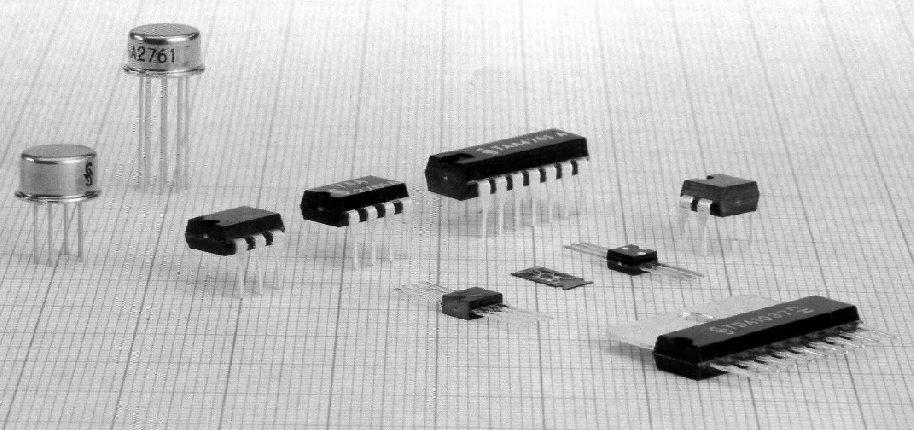
Fig. 7.1: Different integrated circuits
Depending on the way they are manufactured, integrated circuits could
be divided into two groups: hybrid and monolithic. Hybrid circuits have
been around longer. When some transistor is opened, one could find inside
of it's casing a crystal plate whose volume is hundred times smaller than
the casing's. This means two things. First, actual size of the transistor
is very small and, second, if many transistors were placed on a single
non-conducting plate connected in a way to form a certain purpose circuit,
and then encase that altogether in a single package you would get an
instant to use and experiment on circuit with lower price and form factor
than it would be if you made it from regular components yourself (not to
mention the time needed to solder all components together, or to
troubleshoot a faulty component if something cooks up). Solder is replaced
with conducting glues. Resistors are drawn with resistance pastes, and the
plate is then placed inside of the plastic or metallic casing with leads
coming out. Audio-power amplifiers with mark STK, were manufactured like
that.
Today, hybrid circuits are being pushed back by the monolithic
integrated circuits. All components (transistors, diodes, etc.) of a
monolithic circuit are embedded inside of a single tiny silicon plate,
which is then placed inside of a plastic, ceramic, or rarely, metallic
case. Conductive leads, or pins, are one the outside of the case, which
are used for connecting supply, input signal and external components which
cannot be integrated (capacitors, coils, relays, etc.).
Pin placements
for some of the more common packages are on picture 7.2:
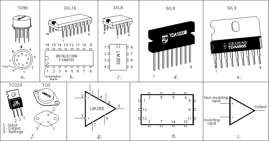
Fig. 7.2: Pin placements and symbols for some common
integrated circuits
As with transistors, integrated circuits which are housed in round
casing (one of them is the TO-99, as on picture 7.2a), angle of view is
from the bottom, which means that schematic depicts pins as they are
facing the viewer (lying on it's back). Small half-round slit, or the
"nose" as often referred to, is used as an orientation help.
Today,
most common found form of an integrated circuit is the chest shaped DIL
(DIL16 and DIL8 are shown on pictures 7.2b and 7.2c). Circuit is viewed
from the top (where are manufacturer's logo and other marks, like model).
Pin counting is circling around the circuit. That means that counting
starts from the "nose's" left side, and from the bottom of the right side
back to the nose.
High power integrated circuits which generate lots of
heat are placed in larger cases with the ability for add a heatsink to
dissipate the temperature. Examples for those circuits are high power
audio-amplifiers with SIL9 case, shown on pictures 7.2d and 7.2e, and the
popular DC voltage stabilizer LM713 in two option casings: TO220 and
TO3.
Symbols used to represent integrated circuits in schematics are on
the pictures 7.2g, 7.2h and 7.2i. Symbol is 7.2g is commonly used to
represent amplifiers. Different digital and impulse integrated circuits
are represented with the 7.2h. Picture 7.2i shows us an important circuit
it is an operational amplifier. Signs + and - are representing inverting
and non-inverting input line. Signal which is to be amplified is brought
between one of the input lines and ground (ground and supply aren't
represented, but are mandatory for the circuit to operate).
Integrated
circuits could be divided in two groups: analog (linear) and digital.
Output voltage of linear circuits is continuous, and follows changes in
the input. Typical representative of linear circuits is an integrated
audio amplifier. When a low frequency source is connected to it's input,
microphone for example, voltage on speaker will vary in the same way as
voltage from the microphone varies. If watched on an oscilloscope,
voltage's signal on the speaker will be the same shape as the mic's
signal, only voltage will be higher depending on the amplification of used
integrated circuit.
It is different situation with digital circuits.
Their output voltage, as all other voltages in their circuitry, is not
continuous. That voltage could be one of only two possible values: zero,
which means that there is zero voltage or one, which is equal to the
voltage of the supplying source.
1. Analog integrated
circuits
While discussing analog circuits, we will look at the LM386
circuit as our example. It has all needed components in single package for
a complete audio-amplifier. Picture 7.3a shows an example of an amplifier
realized using this integrated circuit, which can be used as a complete
low frequency amplifier for a walkman, interphone, cassette player or some
other audio device. It could also be used as a test circuit for different
experiment and troubleshoot situations. These techniques will be discussed
more in forthcoming "Practical ELECTRONICS".
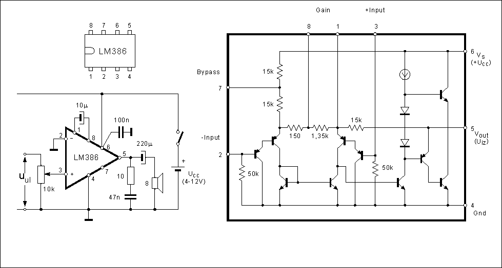
Fig. 7.3: a - LF amplifier using the circuit LM386, b -
LM386 schematic
Schematic of the LM386 is on picture 7.3b. Although it is a
simplified representation of this circuit it clearly points that if it was
devised in discrete technique (from different single components) it would
take us ten transistors, two diodes and eight resistors (one of them is
placed instead of a supply source, represented on the schematic as a
rounded arrow), amplifier devised in this way would be a lot more
expensive, larger and with far worse characteristics than it would be the
case if integrated circuit was used.
Amplifying signal is brought to a
non-inverting input (between the third pin and ground) of the amplifier.
Inverting input (pin 2) is connected to ground. If 10µF was placed between
pins 1 and 8 voltage amplification would be A=200. If this capacitor was
left out, amplification would be A=20. It is possible to achieve any of
the in-between amplification values by adding a resistor to the circuit
and connecting it in series with the capacitor.
One of the essential
components in this circuit is the 100nF capacitor which is placed between
the pin 6 (which is connected to the positive pole of the supply) and
ground. Capacitor used should be ceramic, and should be mounted as close
to the integrated circuit as possible. This is a common practice while
working with all integrated circuits, even when isn't displayed on the
schematic because a capacitor connected between the positive and negative
side of the supply stabilizes the voltage and thus protects the circuit
from the damage which could be inflicted by varying voltage.
2. Digital integrated
circuits
CD4011 will be our "show-and-tell" circuit while learning
the main characteristics of digital integrated circuits. It is a 14 pin
DIL packaged circuit. Pin placement is displayed on picture 7.4a. The view
is, as said previously, as with other DIL packages, from above. Notice the
small half-round slit on one side of the circuit. It is already mentioned
identifier, pin 1 is on it's left side, and pin 14 on it's right side. No
matter how you use this circuit, between pins 7 and 14 are used to connect
a supply (battery or transformer). Negative battery pole is connected to
pin 7. This is a ground, to which all other voltages are measured. All
unused pins should be connected to ground as well. For example, if a logic
circuit with inputs on pins 1 and 2 was unused, those pins would be
connected to pin 7, or ground. Positive voltage is connected to pin
14.
There are four logic NAND gates in the CD4011 circuit. Each one of
them has two inputs and one output. For gate 1 inputs are on pins 1 and 2,
and output is on pin 3. Symbol for NAND gate is displayed on upper part of
7.4b. It's inputs are marked with A and B, and output is marked with an F.
For the sake of simplicity, we will think of it as the upper lef gate of
the CD4011. It's supply is 5V, which means that that is the voltage
between the pin and ground. It also stands true for output voltage. The
same case is when we consider that zero voltage is on one of the
pins.
Lower part of picture 7.4b represents the truth table for a NAND
gate. It shows us what is the output voltage (voltage between F and
ground) with different input states. Because there are only two voltages
in which pins could function, we call them states, with logic zero state
when voltage is zero on that pin, and logic one when voltage on the pin is
5V (actually 5V is given here only as a refference, any voltage, in the
range specified by the datasheet, brought to inputs would, if the
conditions were met, give that voltage on the output , but the essence
remains the same, since there are still only two possible states which
differentiate logic zero and logic one). From what we said above, we can
read the second row of the truth table for this gate as follows: if logic
zero is on both input pins, output is logic one, third row is similar: if
the first input is one, and the second one is zero, output is logic one,
fourth row: if the first input is zero, and the second one is one, output
is logic one. Fifth row is different, since both of it's inputs are one,
the definition of NAND gate states that output is zero. This comes since
NAND gate is derived from the basic AND gate, which gives logic one output
only when both inputs are one, but with added inverter (or a NOT gate)
whose output is always opposite from it's input, whichever of the two
values it is.
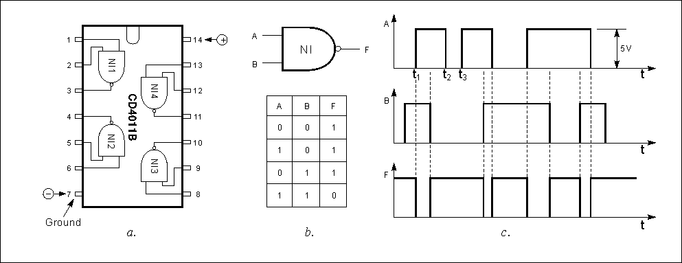
Fig. 7.4: a - 4011 pin placements, b - symbol and the
truth table for NAND gates,
c - voltage behaviour on the inputs and
outputs of the 4011
Logic circuits have many applications, but their main field
is in computer hardware. Picture 7.4c displays what we would see if we
attached an oscilloscope to pins of a logic NAND gate inside of some
computer. Regulated operational voltage of this circuit is 5V. Input A
(upmost diagram) is zero till moment t1 (there is no voltage over it).
Between moments t1 and t2 it is logic zero (voltage is 5V), after it, it
is zero till t3, and so on. Similar voltage impulses (logic ones) occur in
input B as well. Voltage on output F is displayed on the bottom picture.
It has a logic one in those time intervals when at least one input is
equal to zero. When both inputs are one, output is, as said in the truth
table, zero.
Author assumes that those readers which were introduced
with the logical circuits for the first time are suffering a massive
headache, questioning what is exactly the usage of these circuits. Is it
possible to develop anything even remotely functional in amateur labs
using them? There is a simple answer: yes! These circuits have enormous
potential for development of different kinds of homebrewn devices, all
depending on your imagination and persistence. Here's an example, we'll be
making a device which will allow us to turn on any electrical appliance
with a gentle touch of a finger, and which will turn itself off after a
certain amount of time. We will use ordinary 12V light bulb, but if you
use a relay instead of a bulb it would be possible to, for example, turn
on the ventilation fan when you walk out of a bathroom, or hall-light or
some other device, and that will turn that bulb off after some time has
passed.
Using four gates from the picture 7.4a, connected in fashion
depicted on 7.5a, a so called monostable-multivibrator is devised (this
circuit is called a monostable flip-flop also). Notice that there is no
supply on that picture, and that there are no pins 7 and 14. They are left
out for the sake of simplicity, but without some power source circuit
would not operate.
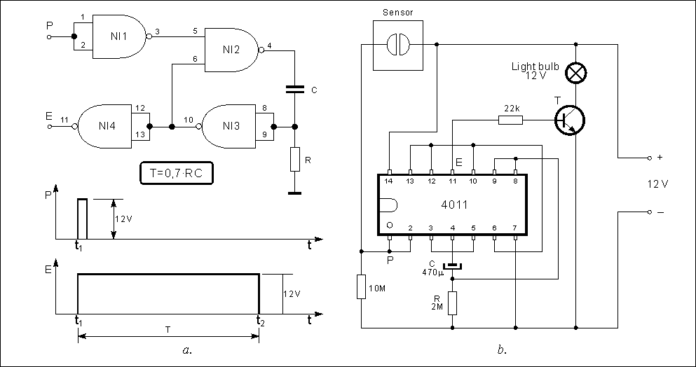
Fig. 7.5: a - monostable multivibrator using four NAND
gates, b - sensor switch using the 4011
Lets dig into the functionalities of this circuit. Both
inputs of NAND1 are connected to each other, so when input P occurs,
output is zero. This logic zero is passed on to NAND2, so no matter what
is on the input 6, output 4 is logic one. This means that, between the
ground and pin, voltage is equal to 12V. Current flows through capacitor C
and resistor R, so capacitor begins to fill. Every empty capacitor behaves
like a short circuit. Because of that, when 12V appears on the pin, it is
also present on the resistor R. It is a voltage between it's upper end and
ground, and that also means with the connected pins 8 and 9. Pin 10 shows
logic zero because of this which is connected to pin 6. From now on, logic
zero on pin 5 is no longer needed because only one input needs to be zero
for output to be logic one. So input P is no longer needed as well. Gates
NAND2 and NAND3 are self sufficiently maintaining logic zero on pin 4. How
long will this last? It depends on the capacitance of the capacitor and on
the resistance of the resistor. As capacitor is filled, voltage on
resistor rises so the current and voltage drop. When this voltage drops to
1/2 of the supply voltage (6V in our case), NAND3 detects zero on it's
inputs, and so logic one appears on pin 10. Since logic one is now on
input 5 (no logic one present on P), and on input 6, output 4 is zero,
capacitor dumps it's charge, and the circuit starts operating again. As we
saw, for a certain period of time, which is equal to T=0.7*RC output of
pin 10 was logic zero. During that time output E (pin 11) is logic one.
For example, if R = 2M? and C=47µF, for time T = 2*10^6*47*10^-6 = 94 s
from the moment impulse on input P subsided, voltage on output E is
12V.
End result of our experiment is on picture 7.5a. Short positive
impulse appearing on P in the moment t1 caused a rather longer lasting
variable impulse on output E.
Schematic on 7.5b displays this circuit
which allows us to light a bulb using four NAND gates interconnected in
the way shown on picture 7.5a.
Sensor itself is devised using two
copper (or some other conducting material) plates glued to some
nonconducting material (plastics, wood, etc.) in close proximity between
each other. So, when we touch with a tip of our finger and by that
connecting two plates, we close the circuit, 12V appear on input P, which
in return conducts that voltage to the output E, resistor R = 22kO
conducts base current and bulb lights. When we remove our finger, output E
will last for 94 seconds, after which it goes to logic zero and the light
goes out.
Transistor T is selected so that it's maximum allowed
collector current is higher than the current of a light bulb.
(Light
bulb's current flow value is acquired by dividing it's power with it's
voltage. For example, if it's power is P = 6W and voltage is U = 12V,
current through the bulb is I = P/U = 6W/12V = 0.5A or higher.
3. Practical examples
Interesting and useful applications, which would demonstrate
properly all possiblities and broad usage of these electronic components
are too much of a scope than could be addressed by this book. So, we will
demonstrate another three circuits, and some others will be covered in
some future issues.
Picture 7.6 shows electric schematic for a stereo
audio-amp using TDA4935. It is a modern integrated circuit with two
independent low frequency amplifiers with a pre-amp, supply stage and an
output stage.
Left and right low frequency signals are marked with UL
and UD, which are brought to two inputs of the amplifier. Beside the amp,
circuit also has a built-in heat and overload protection. Maximum output
power for each of these amplifiers is 15W, so they can be used in stereo
devices of 2x15W output power. There is a possibility for these amplifiers
to be connected as a bridge, to facilitate a 30W mono amp. That schematic
as well as explanations, it's characteristics and practical usage you'll
find out in future issues of "Practical ELECTRONICS".
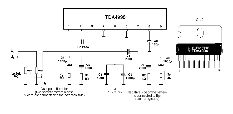
Fig. 7.6: Stereo audio-amplifier using the
TDA4935
Another example is a audio amplifier using a LM386 circuit,
with an additional simple preamp using the transistor BC107. Serially
connected capacitor and resistor between pins 1 and 5 are facilitating low
frequency amplification (around 100Hz) improving characteristics of the
circuit which is important if it is to be used with small speakers.
Capacitor between pin 7 and ground is added on occasions when amplifier
doesn't work properly. Another troubleshooting measure would be replacing
the resistor marked with an asterisk on the schematic. This amplifier
could be used with any low frequency source (gramophone, microphone, some
transformer, etc.), it could also be connected instead of a BC107 on
schematic 4.8, and thus develop a radio-receiver with speaker
reproduction.
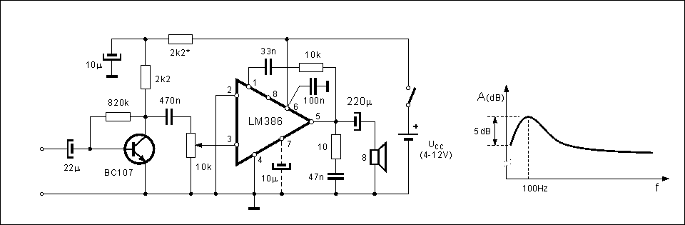
Fig. 7.7: complete audio-amplifier using the
LM386
Third example is a simple alarm device, whose schematic is
on picture 7.8. Base circuit for this device is again the CD4011. It's
gates NAND3 and NAND4 form a 600Hz audio oscillator. This signal is
amplified using BC286 transistor and reproduced using a speaker. To
achieve a 600Hz sound, cut the connection between pins 4 and 8, and
connect pin 8 to pin 9. This makes sound a constant tone. Gates NAND1 and
NAND2 are forming a 4Hz oscillator, whose output is connected to pin 8.
This makes alarm produce repetitive 600Hz sounds with very short breaks.
If you want to use this alarm in your home, on doors for example, you
could make switch S using two brass plates, connected to pins 1 and 7,
which will be adjusted to both a door and a door frame making them conduct
current when doors are closed, so, when door is opened, circuit is
signaled to start the alarm. You could combine this circuit with already
mentioned time interval counter, only instead of a light bulb, you can
connect it to your alarm. This would prevent shutting the alarm if the
door was immediately closed upon entering the room since alarm will sound
until time period T is over.
Frequency of the first oscillator, or
frequency of silent gaps created by the second oscillator are determined
using this formula fi = 0.6/(Ri*Ci). So, to lower those frequencies you
should rise the values of resistors (R1 and R2) or capacitor C1's. If you
were looking a contrary effect, values of those components should be
lowered. It all remains the same for the second oscillator, only resistors
R3 and R4 and capacitor C2 should be used.
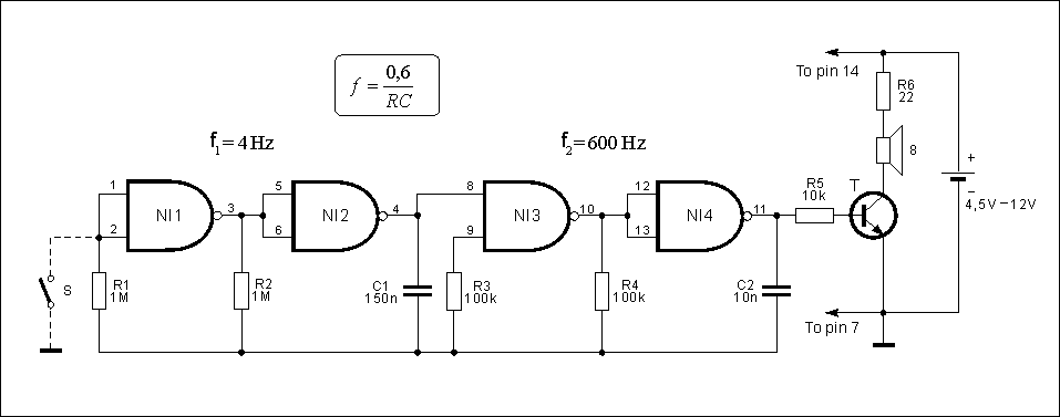
Fig. 7.8: Alarm device using the CD4011
Some other sensor could be used instead of the S switch.
What is important is that it's resistance is very small in ordinary
conditions, and when an alarming situation arises (burglary, fire, flood,
global thermo nuclear war, anything that this alarm is supposed to detect
and announce) it has a very large resistance. For example, if we connected
a photo resistor to the circuit, alarm would be silent while there is
light, but it would sound when the light is off.
Last schematic in this
chapter is an example of a mono FM receiver using the TDA7088T circuit,
which could, along with the SMD components, be housed inside of a
matchstick box along with two miniature batteries for wrist watches.
Schematic is on picture 7.9.
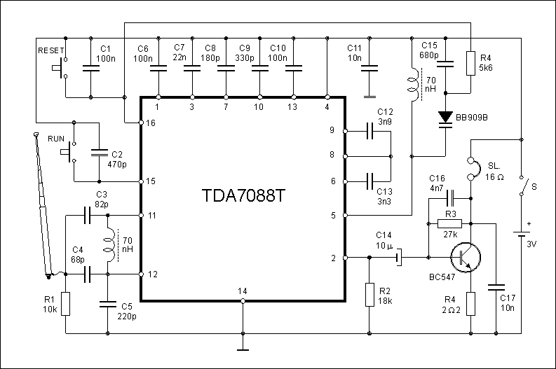
Fig. 7.9: Mono FM radio receiver with an electronic
preset
Tuning to a low frequency station is done automatically by
pressing the RUN switch. That turns on part of the integrated circuit
which is designated for scanning over the given range. When it finds a
station it stays locked on it until some other pressing of the RUN button.
When it reaches 108MHz it waits for the RESET signal which brings it back
to the beginning of the predefined interval
(88MHz).
|